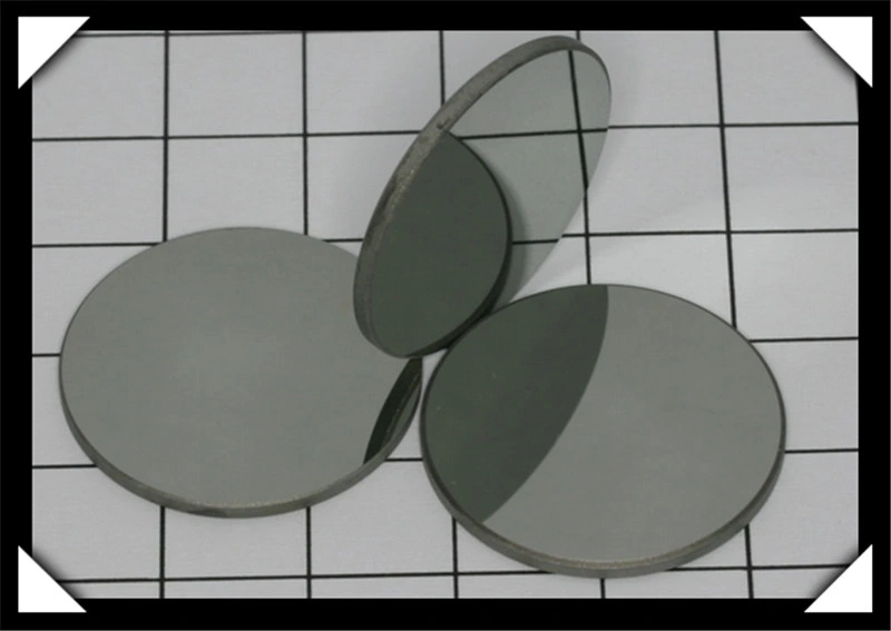
Single crystal (Ge)Germanium Wafer
Ge wafer:
Germanium (Ge) is the preferred lens and window material for high performance infrared imaging systems in the 8-12 um wavelength band. Its high refractive index makes Ge ideal for low power imaging systems because of minimum surface curvature. Chromatic aberration is small, often eliminating the need for correction.
Germanium is most widely used for lenses and windows in IR systems operating in the 2 um - 12 um range. Its transmission is very temperature sensitive, becoming opaque near 100°C. Environment does not cause problems because Germanium is inert, mechanically rugged, and fairly hard.
Germanium is a high index material that is used to manufacture Attenuated Total reflection (ATR) prisms for spectroscopy. Its refractive index is such that germanium makes an effective natural 50% beamsplitter without the need for coatings. It is also used extensively as a substrate for production of optical filters. Germanium covers the whole of the 8-14 micron thermal band and is used in lens systems for thermal imaging. It can be AR coated with diamond producing an extremely tough front optic.
Application as window, lens, beamsplitter, ATR prism or filter in spectrometers and in thermal imaging.
Specifications:
Ge wafer:
Material: |
Ge |
| Dimension Tolerance | +0.0, -0.1mm |
| Thickness Tolerance: | ± 0.1mm |
| Surface quality: | 60/40 |
| Clear Aperture: | >85% |
| Flatness: | λper 25mm |
| Parallelism: | 3' |
| Bevel: | <0.25mm X 45° |
| Coating: | Upon requirement |
General Properties of Germanium Wafer
| General Properties Structure | Cubic, a = 5.6754 Å | ||
| Density: 5.765 g/cm3 | |||
| Melting Point: 937.4 oC | |||
| Thermal Conductivity: 640 | |||
| Crystal Growth Technology | Czochralski | ||
| Doping available | Undoped | Sb Doping | Doping In or Ga |
| Conductive Type | / | N | P |
| Resistivity, ohm.cm | >35 | < 0.05 | 0.05 - 0.1 |
| EPD | < 5x10³/cm2 | < 5x10³/cm2 | < 5x10³/cm2 |
| < 5x10²/cm2 | < 5x10²/cm2 | < 5x10²/cm2 | |
Grades and Application of Germanium wafer
| Electronic Grade | Used for diodes and transistors, | |||
| Infrared or opitical Grade | Used for IR optical window or disks,opitical components | |||
| Cell Grade | Used for substrates of solar cell | |||
| Standard Specs of Germanium Crystal and wafer | ||||
| Crystal Orientation | <111>,<100> and <110> ± 0.5o or custom orientation | |||
| Crystal boule as grown | 1" ~ 6" diameter x 200 mm Length | |||
| Standard blank as cut | 1"x 0.5mm | 2"x0.6mm | 4"x0.7mm | 5"&6"x0.8mm |
| Standard Polished wafer(One/two sides polished) | 1"x 0.30 mm | 2"x0.5mm | 4"x0.5mm | 5"&6"x0.6mm |
| Special size and orientation are available upon requested Wafers | ||||
| 4 inch Ge wafer Specification | ||||
| Doping | P | |||
| Doping substances | Ge-Ga | |||
| Diameter | 100±0.25 mm | |||
| Orientation | (100) 9° off toward <111>+/-0.5 | |||
| Off-orientation tilt angle | N/A | |||
| Primary Flat Orientation | N/A | |||
| Primary Flat Length | 32±1 | mm | ||
| Secondary Flat Orientation | N/A | |||
| Secondary Flat Length | N/A | mm | ||
| cc | (0.26-2.24)E18 | /c.c | ||
| Resistivity | (0.74-2.81)E-2 | ohm.cm | ||
| Electron Mobility | 382-865 | cm2/v.s. | ||
| EPD | <300 | /cm2 | ||
| Laser Mark | N/A | |||
| Thickness | 175±10 | μm | ||
| TTV | <15 | μm | ||
| TIR | N/A | μm | ||
| BOW | <10 | μm | ||
| Warp | <10 | μm | ||
| Front face | Polished | |||
| Back face | Ground | |||
Germanium Wafer Process
Thin Germanium substrates are used in III-V triple-junction solar cells and for power Concentrated PV (CPV) systems.